If you have ever disassembled any electronic devices out of curiosity when you were young, you must have seen Printed Circuit Boards (PCBs). They are the networks that connect various electronic components in circuits and supply power to them. Understanding the PCB fabrication process is crucial for anyone involved in electronics manufacturing or hobbyists who create circuits for fun. This comprehensive guide is for electronics enthusiasts to take a close look at PCB manufacturing, from material selection to assembly techniques.
Materials Used in PCB Manufacturing
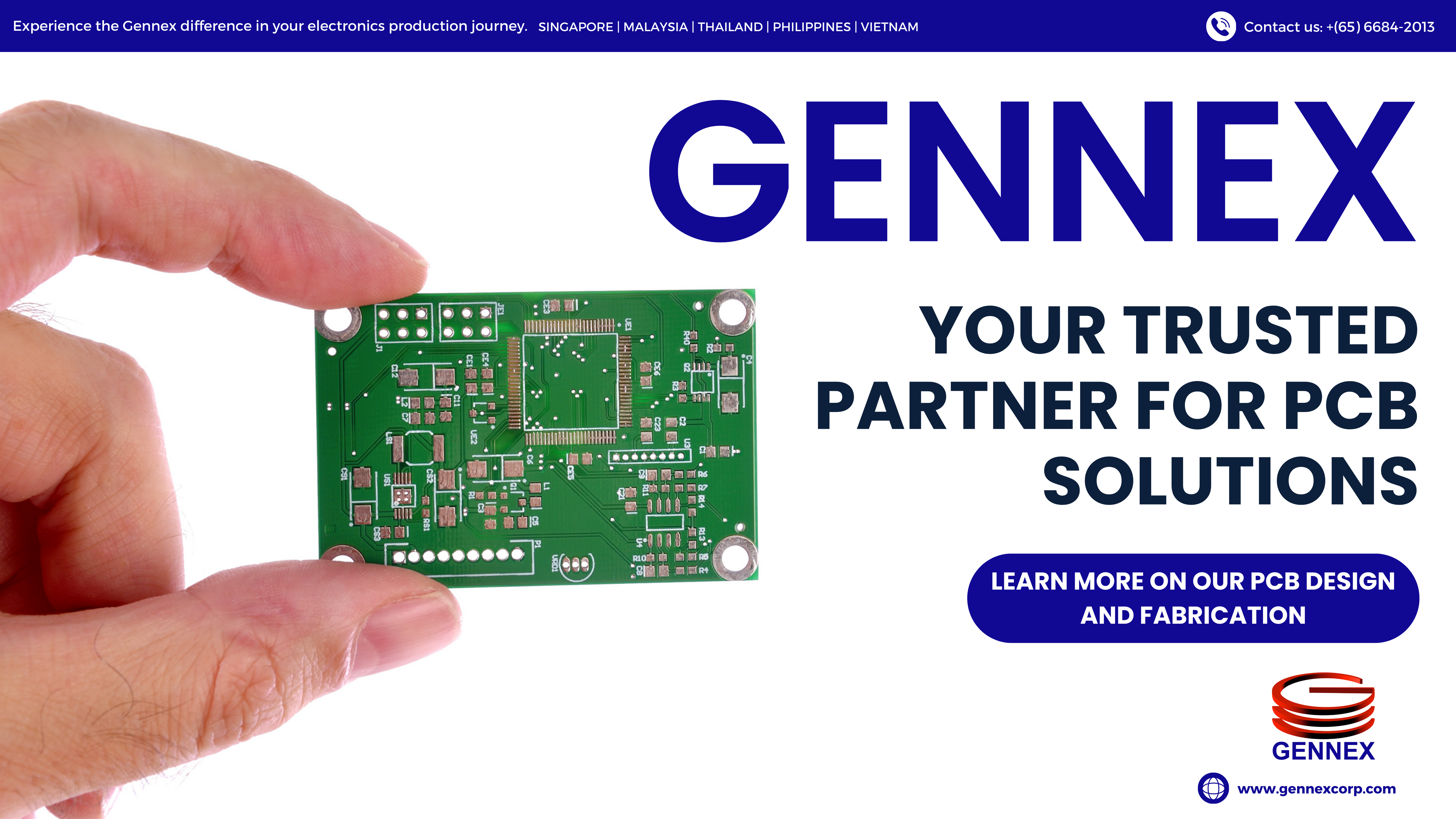
PCBs are typically made of four layers: silkscreen, solder mask, copper, and substrate. The foundation of any PCB is the substrate material, typically a rigid fibreglass known as FR-4. This substrate provides the structural support for the circuitry. Copper foil is then laminated onto the substrate, forming the conductive pathways that link components. The solder mask protects copper traces, and the silkscreen is used to label component locations and polarity markings. Each of these materials plays an important role when it comes to the functionality and durability of the final PCB board you create.
- Silkscreen: Silkscreen, also known as legend printing by some, is applied to the surface of a PCB primarily for labelling and component identification purposes. It is typically printed with white ink onto the board, providing crucial information such as component designators, reference numbers, polarity markings, and logos. Silkscreen enhances the usability of the PCB by making it easier for assemblers and technicians to identify and place components accurately during assembly. Additionally, it contributes to the aesthetics of the board, giving it a professional finish and improving its overall appearance.
- Solder Mask: Solder mask is a layer of protective coating applied over the copper traces on a PCB board. It insulates the copper traces from environmental factors such as moisture, dust, and contaminants, preventing short circuits and corrosion. Solder mask is typically green in colour, although other colours such as red, blue, and black are also used for aesthetic purposes or to denote specific board types.
- Copper: Copper is the primary conductive material used in PCBs. It forms the pathways that connect electronic components and create the circuitry. It is typically laminated onto the substrate in thin sheets, which are then etched to create the desired circuit patterns. Copper offers excellent electrical and thermal conductivity, making it an ideal material for transmitting electrical signals and dissipating heat generated by electronic components.
- Substrate: The substrate which serves as the base material of PCBs is made of a rigid material such as fibreglass reinforced epoxy resin. It is also known as FR-4, which stands for ‘fire retardant’. FR-4 offers excellent dimensional stability, mechanical strength, and resistance to heat and moisture, making it well-suited for a wide range of electronic applications.
What Do You Need to Know about PCB Panel Designing?
Before PCB fabrication begins, a proper PCB panel design that optimises material usage must be created. PCB panel designs may involve arranging individual circuit boards on a larger panel to function simultaneously. Therefore, it is important to carefully consider factors such as panel size, spacing between boards, and routing channels for cutting the panels apart after fabrication. The most important point for you to keep in mind is that efficient PCB designs help minimise the waste of energy, and they can also reduce production costs.
Assembly Techniques of PCB Parts
Once a PCB is fabricated, the next step is assembling the components. This process is known as PCB assembly or soldering. It involves placing components on the board and soldering them into place. There are two primary methods of PCB assembly: through-hole and surface mount. Through-hole assembly involves inserting component leads through holes in the board and soldering them to copper pads on the opposite side. Surface mount assembly, on the other hand, involves soldering components directly onto the surface of the board. In general, surface mount assembly is known to offer greater component density and is well-suited for miniaturised electronics.
Special Features and Applications of PCBs
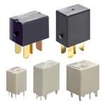
The versatility of PCBs is vast, finding applications across diverse industries and contexts. From consumer electronics to aerospace endeavours, PCBs serve as the backbone of many innovations. Carefully designed, compact PCBs make them indispensable in devices ranging from smartphones and computers to medical equipment and industrial machinery. Moreover, the multi-layer construction techniques involved in PCB manufacturing have unlocked new possibilities in electronic design, facilitating the integration of increasingly complex circuitry into miniature spaces.
Get Your PCBs Manufactured by Industry Leaders
Whether you’re an electronics enthusiast embarking on a DIY project or a seasoned engineer spearheading cutting-edge research, understanding the fundamentals of PCB fabrication is important. However, PCB manufacturing requires extensive knowledge and experience. Without proper techniques, tools, and equipment, it is impossible to design well-functioning, durable PCBs. If you are looking for a reliable electronic components distributor to get PCBs fabricated, look no further than Gennex. With a commitment to quality and innovation, we offer you the best options that fit perfectly with your unique requirements.