Navigating PCB design complexities can be overwhelming. Subpar designs lead to setbacks and financial strains.
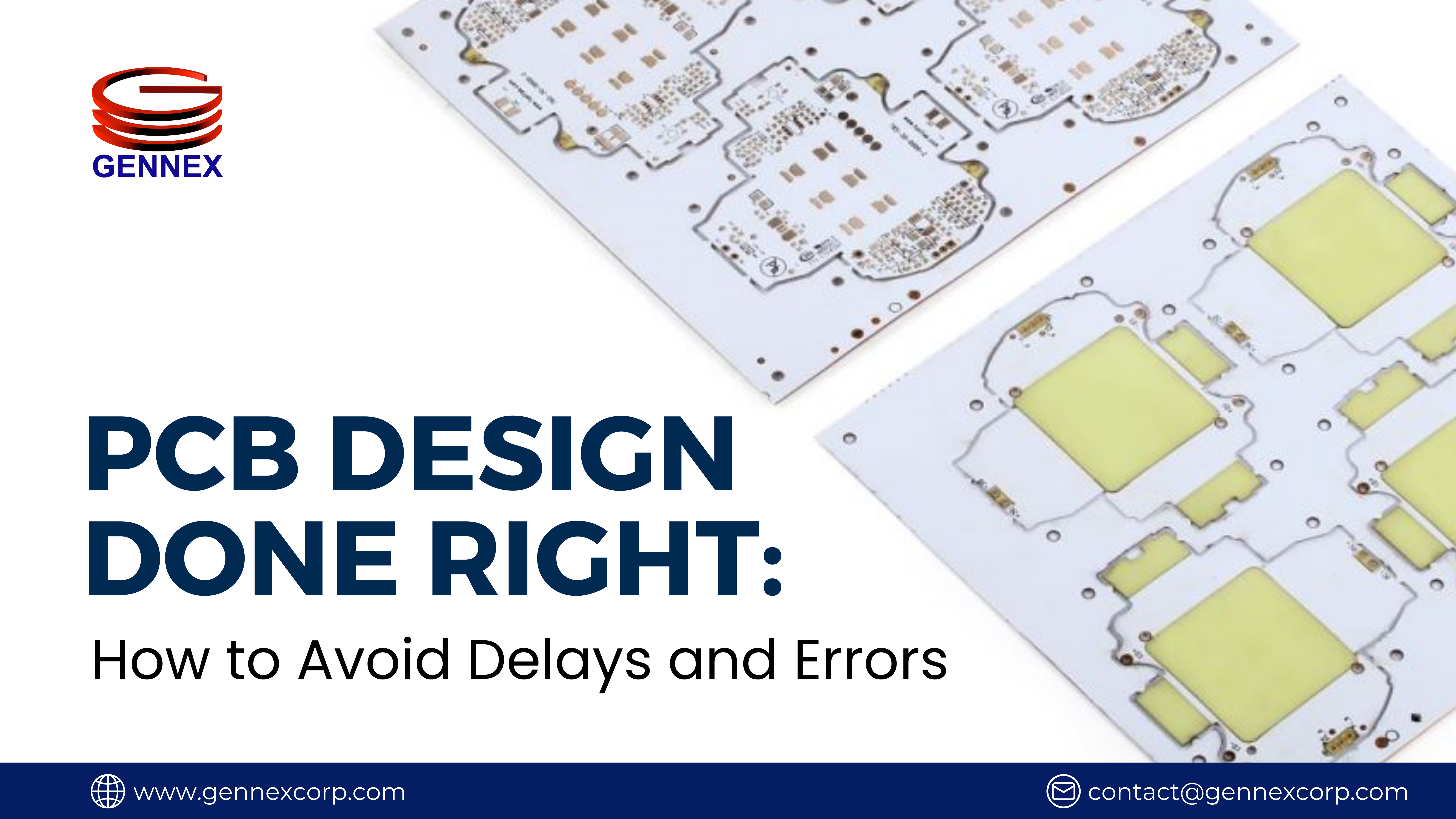
The Critical Importance of Efficient PCB Design
In the world of electronics manufacturing, efficient PCB design is not just a luxury—it’s a necessity. As you navigate the complex landscape of product development, understanding the critical role of PCB design can make or break your project’s success.
Precision and Complexity: The Dual Challenges
PCB design demands an intricate balance of precision and complexity. Your designs must accommodate increasingly sophisticated components while adhering to strict spatial constraints. This delicate dance requires not only technical expertise but also a keen eye for detail and a forward-thinking approach to potential manufacturing issues
Time: The Unforgiving Factor
In today’s fast-paced market, time-to-market can be the difference between leading the pack and falling behind. Efficient PCB design significantly reduces development cycles, allowing you to iterate quickly and respond to market demands. By streamlining your design process, you can avoid costly delays and stay ahead of your competition.
The High Cost of Errors
Subpar PCB design can lead to a cascade of problems downstream. Manufacturing errors, component failures, and performance issues can all stem from inadequate design practices. These mistakes not only inflate costs but can also damage your brand’s reputation. Investing in efficient PCB design is an investment in your product’s reliability and your company’s future.
Embracing Advanced Design Capabilities
To meet these challenges head-on, you need access to cutting-edge design tools and expertise. Advanced PCB design software, coupled with experienced designers, can help you navigate complex layouts, optimize signal integrity, and ensure manufacturability. By leveraging these resources, you can create designs that are not just functional, but optimized for performance and cost-effectiveness.
Common Pitfalls of PCB Design and How to Avoid Them
When designing printed circuit boards (PCBs), you may encounter several challenges that can impact your project’s success. Understanding these common pitfalls and implementing strategies to avoid them is crucial for efficient PCB design and manufacturing.
Inadequate Component Spacing
One of the most frequent mistakes in PCB design is insufficient spacing between components, which can lead to several types of issues, such as manufacturing difficulties, potential short circuits, component placement difficulties, and overheating issues. To prevent this, ensure you follow recommended clearance guidelines and consider thermal management requirements when placing components.
Improper Signal Routing
Inefficient signal routing can result in timing delays, electromagnetic interference (EMI), and signal integrity problems. To avoid this, implement best practices such as using appropriate trace widths, maintaining proper signal return paths, and minimizing crosstalk between high-speed signals. Consider utilizing advanced routing techniques like differential pairs for sensitive signals, and the performance of Design rule checks (DRC) is another helpful tool to guarantee the PCB’s integrity and the electrical product’s overall success.
Neglecting Power Distribution
Inadequate power distribution can cause voltage drops and noise issues across PCB. To mitigate this, design a robust power distribution network with sufficient copper thickness, create a layer for the ground and power plane and ensure proper placement of bypass capacitors near power-hungry components, if necessary.
Overlooking Manufacturing Constraints
Failing to consider manufacturing limitations can lead to production delays and increased costs. To avoid this pitfall, familiarize yourself with your manufacturer’s capabilities and design rules. These constraints include a wide range of characteristics, such as minimum trace widths, and spacing, drill sizes, and board edge clearances. Applying these specifications is key to creating a design that satisfies electrical performance requirements and complements the production facilities’ physical and manufacturing capabilities.
Insufficient Documentation
Incomplete or unclear documentation can result in misinterpretations and errors during manufacturing. To prevent this, create comprehensive design documentation, including detailed bill of materials (BOM), assembly drawings, and fabrication notes. Clearly communicate any special requirements or critical dimensions to ensure accurate production.
By being aware of these common pitfalls and implementing strategies to avoid them, you can significantly improve your PCB design process, reduce errors, and minimize production delays. Remember that partnering with experienced PCB design service providers can further enhance your ability to navigate these challenges successfully.
The Costly Consequences of Subpar PCB Design
When you compromise on PCB design quality, you’re setting yourself up for a cascade of costly repercussions. Subpar design practices can lead to significant setbacks in your product development timeline and inflate your manufacturing expenses. Let’s explore the potential pitfalls of inadequate PCB design and why investing in quality from the outset is crucial.
Delays and Rework Cycles
Poor PCB design often results in multiple revision cycles, each eating into your valuable time-to-market. You may find yourself caught in a frustrating loop of design tweaks, prototype testing, and error correction. These delays not only push back your product launch but can also give competitors an edge in the market.
Manufacturing Challenges and Increased Costs
Flawed designs frequently translate to manufacturing headaches. You might encounter issues like:
- Incompatibility with automated assembly processes.
- Increased scrap rates due to design-related defects.
- The need for manual rework, driving up labor costs.
- Incorrect material selection, fails to meet optimal performance.

Performance Issues and Customer Dissatisfaction
Suboptimal PCB design can lead to functionality problems in your final product. You may face issues such as:
- Improper layout design which can cause signal integrity problems causing intermittent failures
- Thermal management challenges leading to overheating.
- EMI/EMC compliance failures requiring costly redesigns.
These performance issues can damage your brand reputation and result in customer returns, and lost future business opportunity.
Regulatory Non-Compliance and Legal Risks
In today’s stringent regulatory environment, PCB design errors can lead to non-compliance with industry standards. You might face:
- Costly certification delays
- Potential legal liabilities from product failures
- Market access restrictions due to non-conformance
By prioritizing quality in your PCB design process, you can avoid these costly pitfalls and ensure a smoother path from concept to market-ready product.
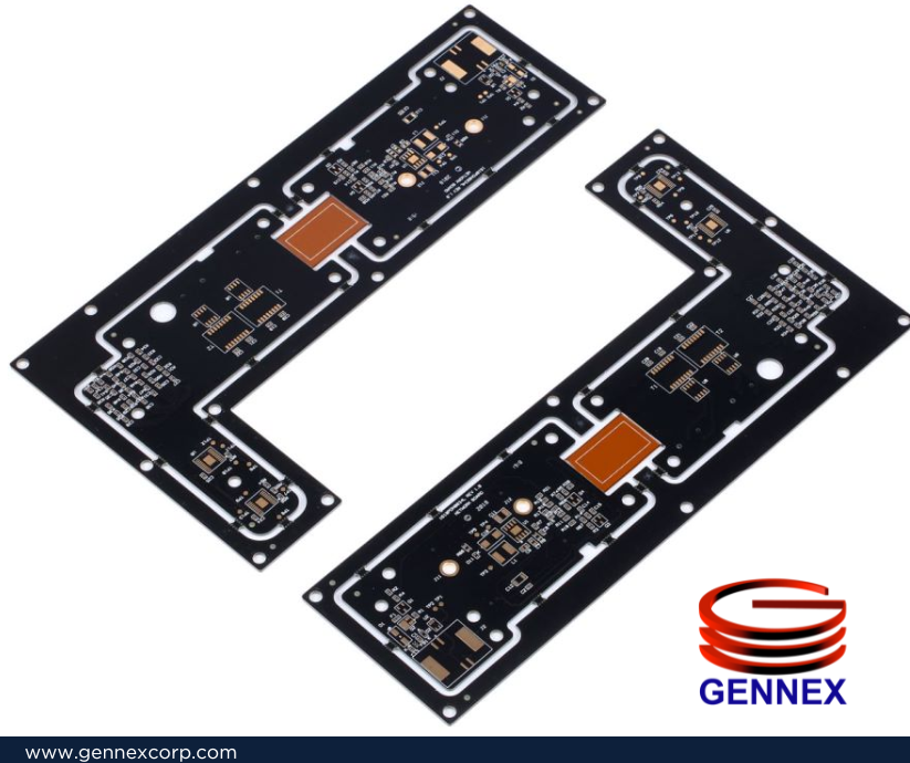
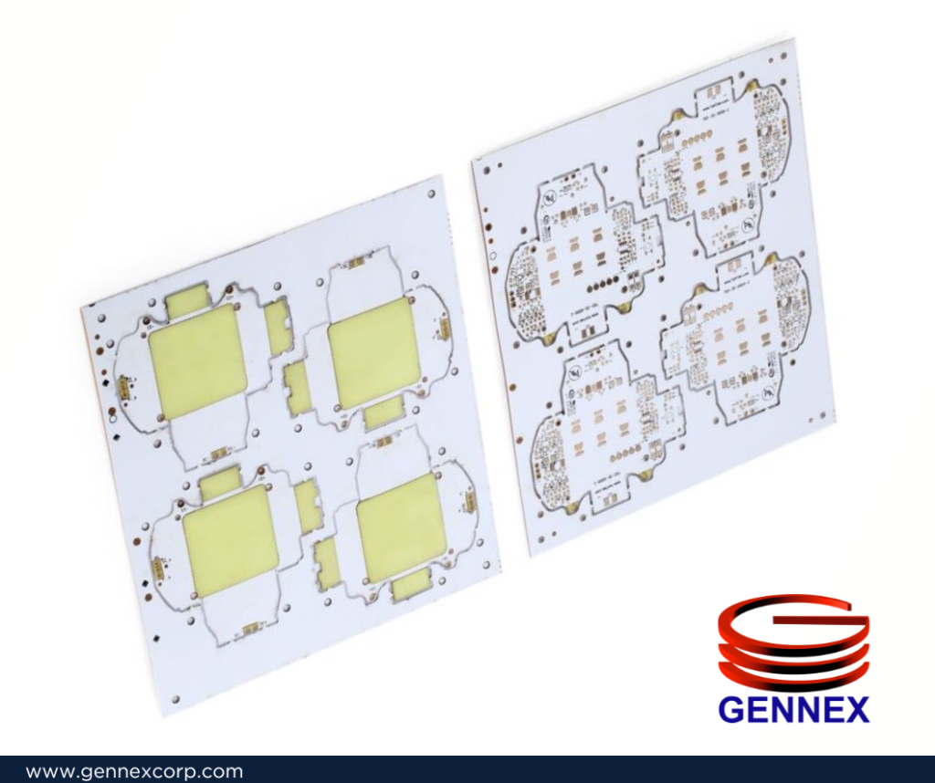
Optimizing Your PCB Design Process With Gennex

A team, fully equipped with a comprehensive suite of tools and software for PCB design can effortlessly deliver and create complex multi-layer boards.
The intuitive interface allows you to visualize your design in real-time which can produce PCB products efficiently.
Tapping into Expert Knowledge
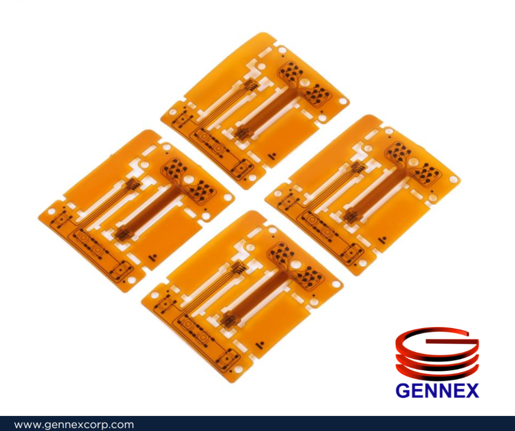
When you partner with Gennex, you gain access to a wealth of expertise across various PCB types. Their team of seasoned engineers can guide you through the intricacies of high-speed digital designs, RF layouts, or flexible PCBs. This collaborative approach ensures that your designs are not only functional but also optimized for manufacturability and performance.

One of the most critical stages in PCB design is the creation of accurate Gerber files. Gennex’s efficient Gerber design services can save you valuable time and reduce the risk of manufacturing errors. With a knowledgeable and thorough understanding team that is keen on the different factors contributing to manufacturing PCB, we facilitate a smoother transition from design to production.

By leveraging Gennex’s quick turnaround capabilities, you can significantly reduce your product development cycle.
Their streamlined processes and dedicated design teams work in tandem to deliver high-quality PCB designs in a fraction of the time it might take in-house. This acceleration can give you a competitive edge in the market, allowing you to launch your products faster without compromising on quality or reliability.

Partner with Gennex
We have the solution.
Gennex ensures that your PCB designs meet the highest standards of reliability and performance.
Contact Gennex Expert Engineers