Your Trusted 24 Hours Business Service Provider !
The Future of Burn-in Testing: AI, 5G, and Advanced Packaging
Smiths Interconnect is at the forefront, pioneering innovations like the Da Vinci sockets, designed specifically for AI chip testing.


Understanding Burn-in Testing: Its Importance in AI and 5G
The Critical Role of Burn-in Testing
As we navigate the rapidly evolving landscape of artificial intelligence (AI) and 5G technologies, the importance of burn-in testing cannot be overstated. This rigorous process is essential in ensuring the reliability and durability of integrated circuits (ICs), which form the backbone of these cutting-edge advancements. At its core, burn-in testing involves subjecting semiconductor devices to elevated temperatures and voltages to simulate the stresses they will encounter in real-world applications. This proactive approach helps identify potential defects early, thus preventing failures in the field. Given the immense computational demands and high-speed data requirements of AI and 5G, the stakes for robust IC reliability testing have never been higher.
Meeting the Demands of AI and 5G
In the context of AI and 5G, the complexity of semiconductor burn-in processes has increased significantly. The need for enhanced burn-in test sockets, especially for High Bandwidth Memory (HBM) applications, is critical. These sockets must accommodate the intricate designs of next-generation chips while maintaining effective thermal management and signal integrity. Smiths Interconnect, a pioneer in this field, has responded with innovations like the Da Vinci sockets specifically designed for AI chips. These solutions not only support the demanding requirements of AI and 5G but also underscore the evolving role of burn-in testing in ensuring the performance and longevity of semiconductor devices in these frontier technologies.
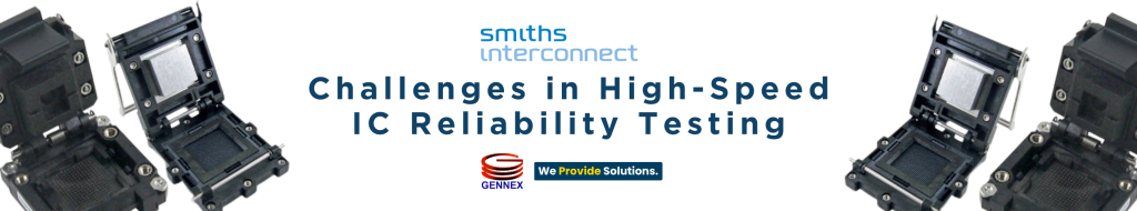
Challenges in High-Speed IC Reliability Testing
Navigating High-Speed IC Complexity
The evolution of high-speed integrated circuits (ICs) introduces complexities that significantly challenge traditional reliability testing methodologies. As circuits become increasingly intricate, the demands on burn-in testing intensify, necessitating innovative approaches to ensure durability and performance.
In particular, high-speed ICs require precision engineering to mitigate issues such as signal integrity and thermal management, which are crucial for maintaining operational efficiency over time.
The Role of Burn-in Test Sockets
Burn-in test sockets specifically designed for High-Bandwidth Memory (HBM) and similar advanced technologies play a pivotal role in this landscape. These sockets must accommodate the stringent requirements of high-speed ICs, offering robust connectivity while minimizing signal loss.
The complexity of these testing environments necessitates sockets that can sustain high frequencies and temperatures, ensuring that ICs deliver consistent performance under stress.
Adapting to 3D Packaging Challenges
With the advent of 3D packaging technologies, the challenges further compound. Three-dimensional packaging introduces unique thermal and mechanical stresses that traditional semiconductor burn-in processes might not adequately address. Engineers now need to devise testing methodologies that account for these multidimensional stress factors, adapting burn-in testing to ensure comprehensive IC reliability testing.
Innovative Approaches
Smiths Interconnect leads the charge in this domain with cutting-edge solutions like the Da Vinci sockets. These innovations are tailored for AI chips, illustrating how forward-thinking designs can transform the reliability testing landscape, ensuring that high-speed ICs meet the rigorous demands of modern applications.
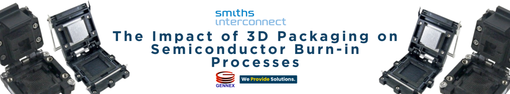
The Impact of 3D Packaging on Semiconductor Burn-in Processes
Innovating for the Future: Smiths Interconnect's Da Vinci Sockets for AI Chips
- Meeting the Demands of Next-Gen Technology
As the industry embraces the capabilities of 5G and AI, the integration of advanced packaging techniques becomes essential. Smiths Interconnect’s innovations, such as the Da Vinci sockets, address the unique challenges posed by these technologies. By refining the semiconductor burn-in process, these sockets not only meet current demands but also anticipate future advancements in chip design and functionality. This proactive approach positions Smiths Interconnect as a leader in adapting burn-in testing to the needs of modern and future technologies.
- Revolutionizing Burn-in Testing with Da Vinci Sockets
In the rapidly evolving landscape of semiconductor technology, Smiths Interconnect stands at the forefront with its innovative Da Vinci sockets designed specifically for AI chips. This cutting-edge solution paves the way for more efficient burn-in testing, a critical process ensuring the reliability and longevity of integrated circuits (ICs). As AI applications demand more from semiconductor devices, the need for robust burn-in test sockets becomes increasingly crucial. These sockets are engineered to withstand the demanding conditions of high-speed IC reliability testing, particularly for advanced high bandwidth memory (HBM) devices
- Enhancing IC Reliability Testing
Smiths Interconnect’s Da Vinci sockets offer a significant leap in IC reliability testing methodologies. By accommodating the unique needs of AI-driven chips, these sockets ensure that semiconductor burn-in processes are both thorough and efficient. The Da Vinci sockets are marked by their precision and ability to handle the elevated temperatures and electrical stresses associated with AI chip testing. This results in a more reliable burn-in procedure, ultimately leading to higher quality end products with enhanced performance and durability.
Burn-in Test Sockets for HBM: Meeting Evolving Requirements in Advanced Technology
- Innovations in Burn-in Testing
Companies like Smiths Interconnect are spearheading advancements in this field, offering cutting-edge solutions such as the Da Vinci sockets for AI chips. These innovations are tailored to meet the unique demands of modern ICs, facilitating seamless integration into high-performance computing environments. By leveraging advancements in burn-in test sockets, manufacturers can ensure that their products meet the highest standards of reliability, thus supporting the rapid growth of AI and 5G technologies.
- The Role of Burn-in Test Sockets
In today’s fast-paced semiconductor industry, ensuring the reliability of high-bandwidth memory (HBM) integrated circuits (ICs) has become paramount. Burn-in test sockets play a crucial role in this process. These sockets are designed to expose ICs to various stresses, such as temperature fluctuations and electrical loads, to weed out potential failures early in the production phase. This proactive approach to IC reliability testing not only enhances product dependability but also mitigates costly post-deployment failures.
- Adapting to Changing Needs
The evolution of advanced technologies like AI and 5G demands that burn-in processes keep pace. As HBM technology becomes more sophisticated, so do the burn-in testing requirements. Test sockets must now accommodate smaller pitch sizes and higher pin counts, while maintaining excellent signal integrity and thermal management. These challenges necessitate continuous innovations, ensuring that the semiconductor burn-in process remains robust and effective.

services
Meet us at SEMICON 2025
Discover the Future of Burn-in Testing
In the ever-evolving landscape of semiconductor technology, SEMICON 2025 offers an unparalleled opportunity to explore the latest innovations in burn-in testing. As industry leaders gather to exchange insights and unveil cutting-edge advancements, you will gain valuable perspectives on how AI and 5G are reshaping integrated circuit (IC) reliability testing.
The future beckons with the promise of more efficient and effective testing methodologies, and SEMICON 2025 is your gateway to this horizon.
Engage with Industry Pioneers
Join us at SEMICON 2025 to engage with pioneers in the field who are driving the evolution of semiconductor burn-in processes.
Whether you’re interested in the enhanced capabilities of burn-in test sockets for high-bandwidth memory (HBM) or the latest in 3D packaging technologies, this event is tailored to meet your interests. Our experts will be on hand to discuss the challenges and opportunities that lie ahead, providing you with the tools and knowledge to stay ahead in this competitive industry.
Experience Smiths Interconnect Innovations
At our booth, you will have the chance to experience firsthand the innovative solutions offered by Smiths Interconnect, including the acclaimed Da Vinci sockets designed for AI chips.
These advanced solutions underscore our commitment to advancing IC reliability testing and ensuring that your semiconductor processes are optimized for future demands. We invite you to join us at SEMICON 2025 to witness how these technologies can transform your approach to burn-in testing.